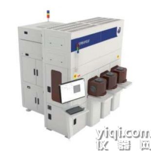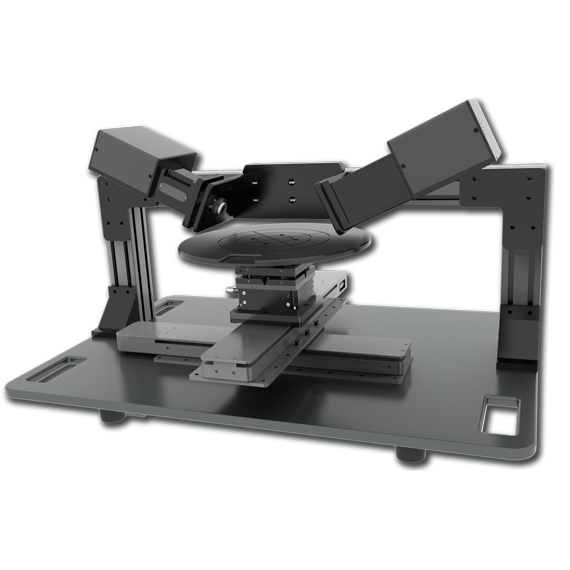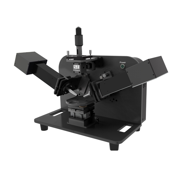

Different tools:
- SE-2xxx-全自動測試平臺
- SE-1100-適于測試柔性村底材料
- IRSE-紅外光譜型橢偏儀
- EP-橢偏測孔隙率
- SE-1000-低成本手動測試平臺
- LE-103PV-激光型橢偏儀
Application:
Photonics:
- LED, AIGaN, GaN, InP, GaAs
- Reflective Coatings, ARC, ll-V devices(EEL, VCSEL, ECL)
- MEMS
- Sol-Gel.
Photovaltage
- Thin films and silicon solar cell, Nanostructure Cells
- Transparent conductive oxide, Nano dots, Nanowires, CNT
Organics:
- OLED.OPV.Sensors. OTFT
Semiconductors:
- High-k, Gate Oxide , Nitride oxide , Low-k
- Interconnects . Lithography thin films
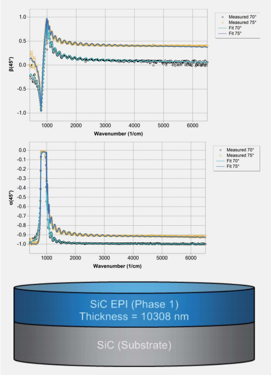
- Epi-layers :SOl,SiGe ,Strained Si. SiC, Poly
Flat Panel Displays:
- TFT-LCD.LTPS.IGZO,OLED, electrochromic layers
General:
- Ferroelectric materials(BST.SBT.PZT
- Fuel Cells .SOFC ,Porous electrode
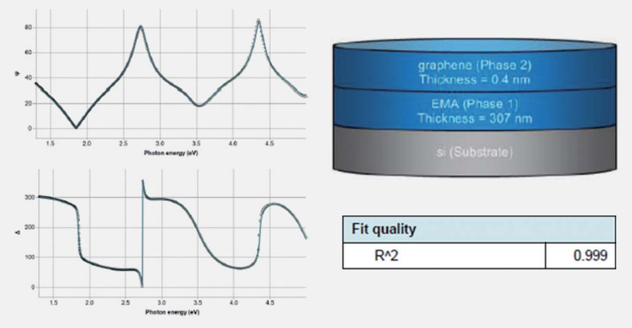
- Graphene
- 3D materials , periodic structures
 |  |
 |